
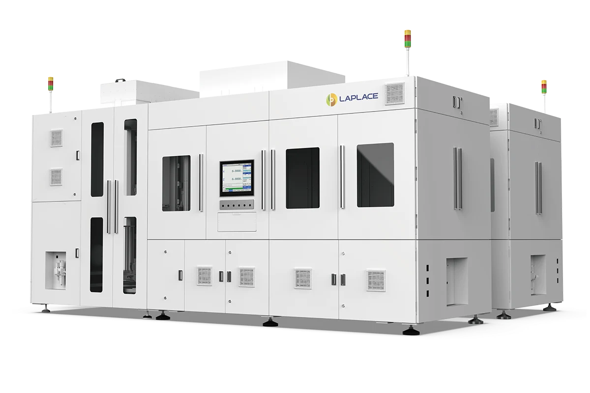
Primarily used in solar cell manufacturing for selective thinning of the polysilicon (Poly-Si) layer on the rear side of the cell. Its main functions include:
Reducing parasitic light absorption. Optimizing electrical performance. Releasing residual stress. Achieving patterned thinning. This equipment is typically integrated with wet etching or plasma repair processes to ensure the surface quality of the thinned Poly-Si layer while preventing damage to the underlying tunnel oxide layer (SiO₂). It is a key process tool for enhancing solar cell efficiency and performance.
Poly Thinning Function
● Principle: Utilizes ultra-fast laser to open the rear side PSG (phosphosilicate glass), followed by a wet process to achieve polysilicon thinning.
● Effect: Reduces parasitic light absorption by the rear side polysilicon, thereby lowering costs and improving efficiency. According to data from LAPLACE, mass production cell efficiency increases by 0.15%+, and module power increases by 4W+.
Other General Functions
● High Stability: Uptime ≥ 99%, breakage rate ≤ 0.02% for 18X, ≤ 0.03% for 210; MTBF ≥ 800 h, MTTR ≤ 1 h.
● Strong Compatibility: Compatible with 18X – 210mm wafers; wafer thicknesses 110 – 220 µm. Laser power ≥ 100 W, power stability ≤ 2%, pattern precision ± 15 µm, repeatability precision ± 10 µm.
● High Degree of Automation: Laser processing via galvo scanning. Offline or inline production can be realized according to customer requirements, facilitating integration with other equipment and enhancing the automation level of the production process.
