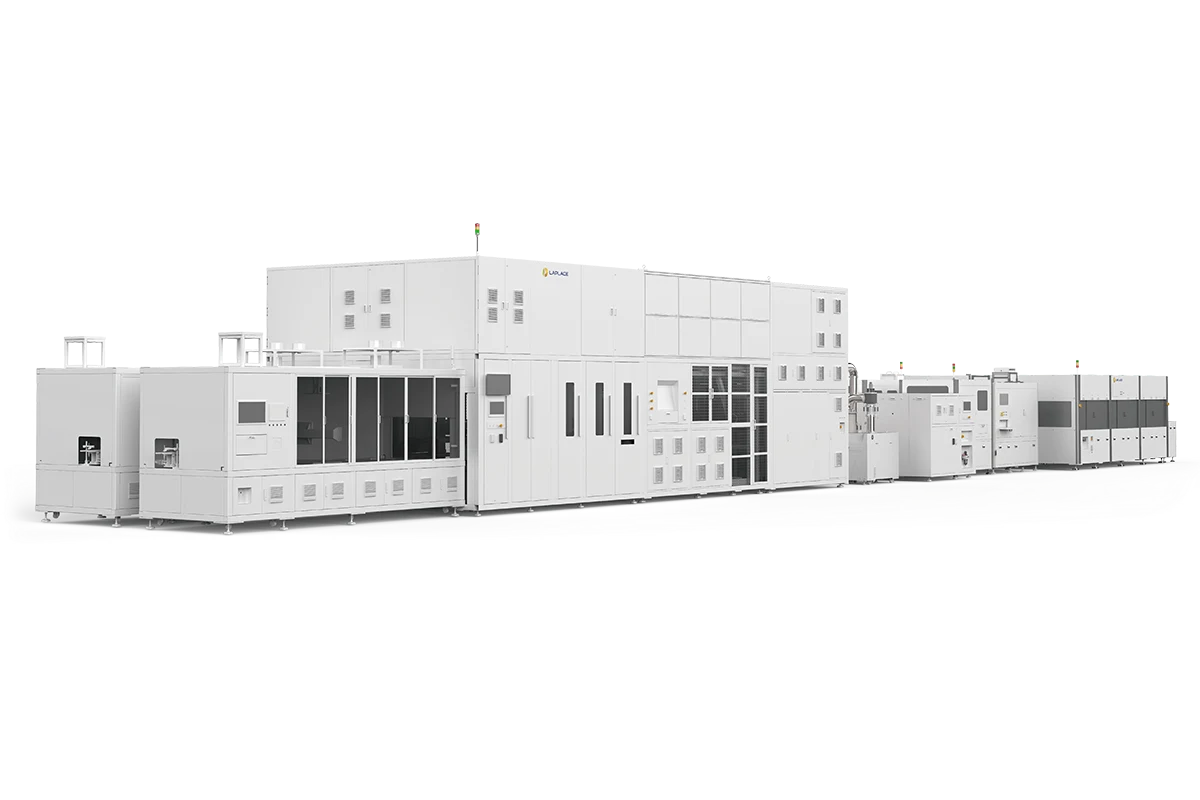
Primarily used in solar cell manufacturing, its core function is to deposit a passivation layer on the edge of solar cells to enhance their performance and stability.
1.Laser dicing function: Precisely controlled heating via laser combined with localized cooling creates a significant temperature gradient within the silicon wafer. When the thermal stress reaches the fracture threshold, the material breaks, and the crack propagates along the thermal gradient induced by the laser beam path, resulting in complete separation of the substrate. This function can process wafer sizes of 18X – 230 mm and thicknesses of 110 – 230 µm, with throughput ≥ 12,000 pcs/h, breakage ≤ 0.02% @18X, ≤ 0.03% @210, and uptime ≥ 98.5% .
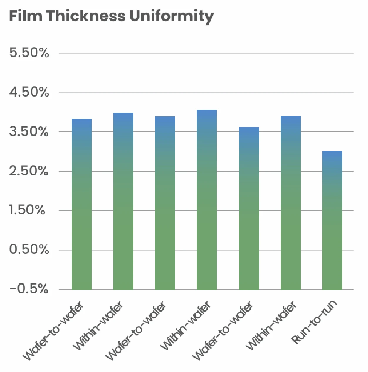
2.Edge passivation function: Utilizes laser non-destructive cutting technology to singulate cells, while simultaneously employing an Atomic Layer Deposition (ALD) process to deposit an AlOx passivation layer on the laser-cut edges, suitable for TOPCon cell applications. Uptime is 99%, with loading capacity of 21,600 half-cut cells per tube. Film thickness uniformity: within-wafer & wafer-to-wafer ≤ 7%, run-to-run ≤ 3%. Features a 4 segment thermal field with 12 zones of independent temperature control, compatible with 400°C annealing process. Process precursors: TMA + water.
3.Testing and sorting function: Equipped with AOI, IV testing, EL testing, it can detect defects such as edge chipping, stains, and foreign objects. Voltage test resolution: 0.0001 V; current test resolution: 0.0001 A. IV dynamic stability < 0.05%, static stability < 0.02%; each sweep EFF max range ≤ 0.05%. Minimum detectable EL defect size: 0.5 mm × 0.5 mm. Sorting capability ≥ 120 bins (single side). Throughput for full cells: 8,500 pcs/h; uptime ≥ 98.5% .
4.Overall performance advantages: Employs advanced atomic layer deposition technology with a tube-type temporal structure, completely isolating reactant sources for pure ALD reaction without CVD components, ensuring film uniformity, density, and refractive index. Features integrated process temperature annealing to reduce film thickness risk, significantly improving cell performance (conversion efficiency) and reliability. The system is rationally designed with a high degree of automation, enabling long-term stable operation, reduced equipment downtime, and increased production efficiency. Additionally, the system offers excellent compatibility and scalability to meet diverse customer requirements and adapt to future technology upgrades and capacity expansion.