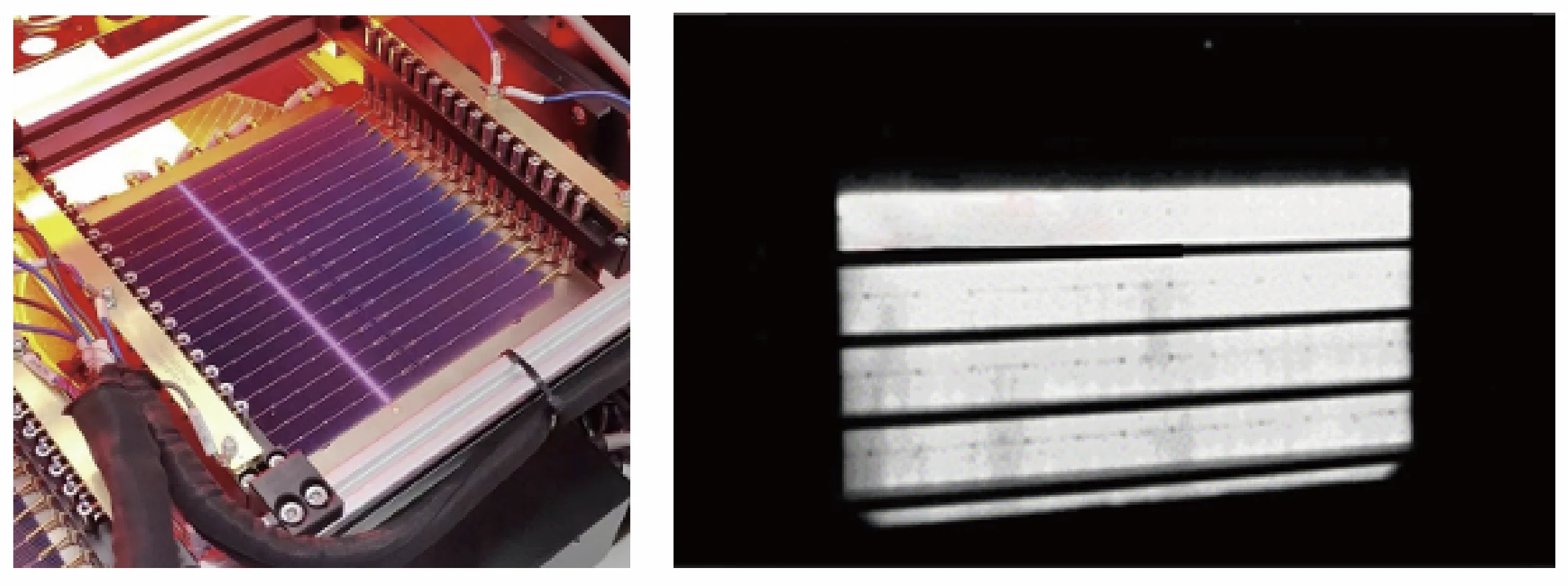
Primarily used to optimize the contact between metal and semiconductors, reducing contact resistance to enhance cell conversion efficiency.
1.Precise destruction of passivation layer: Utilizes laser-induced localized carriers to form a high current density, precisely destroying the local passivation layer to form a silver-silicon alloy contact. This provides an excellent interface for metal contact without damaging the silicon wafer substrate.
2.Optimized metal contact and reduced resistance: Laser-induced processing promotes excellent contact between the metal and silicon wafer, effectively reducing metal-semiconductor contact resistance, thereby enhancing fill factor and conversion efficiency. LAPLACE LIM equipment can achieve an efficiency gain of ≥ 0.3% abs.
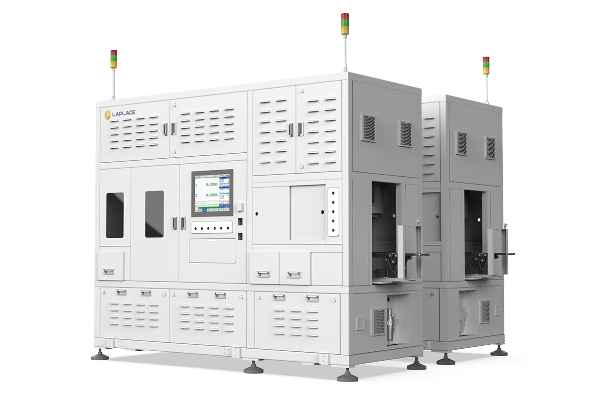
3.High throughput: Employs dual-station design for simultaneous laser processing. Processing. Throughput > 9600 pcs/h for 18X; > 9000 pcs/h for 210.
4.High stability and low breakage rate: Reliable operation with an uptime ≥ 98.5%. Low breakage rate: ≤ 0.02% for 18X and ≤ 0.03% for 210.
5.Strong compatibility: Compatible with various wafer sizes and adaptable to multiple formats including TOPCon full cells, multi-cut cells, and 0BB cells.
6.Process monitoring and NG wafer rejection: Features real-time monitoring of process voltage and current, enabling precise rejection of NG wafers to ensure product quality consistency.
7.Flexible laser processing method: Standard configuration includes area scan solution using a large square spot to process the cell surface, featuring low tuning difficulty, high stability and compatibility, and maintenance-free optical path.
8.Process expandability: Compatible with secondary LIM for full cells and multi-cut cells. Compensates for insufficient primary LIM processing or degradation after other processes through differentiated laser treatment, providing an additional efficiency gain of 0.05% abs.