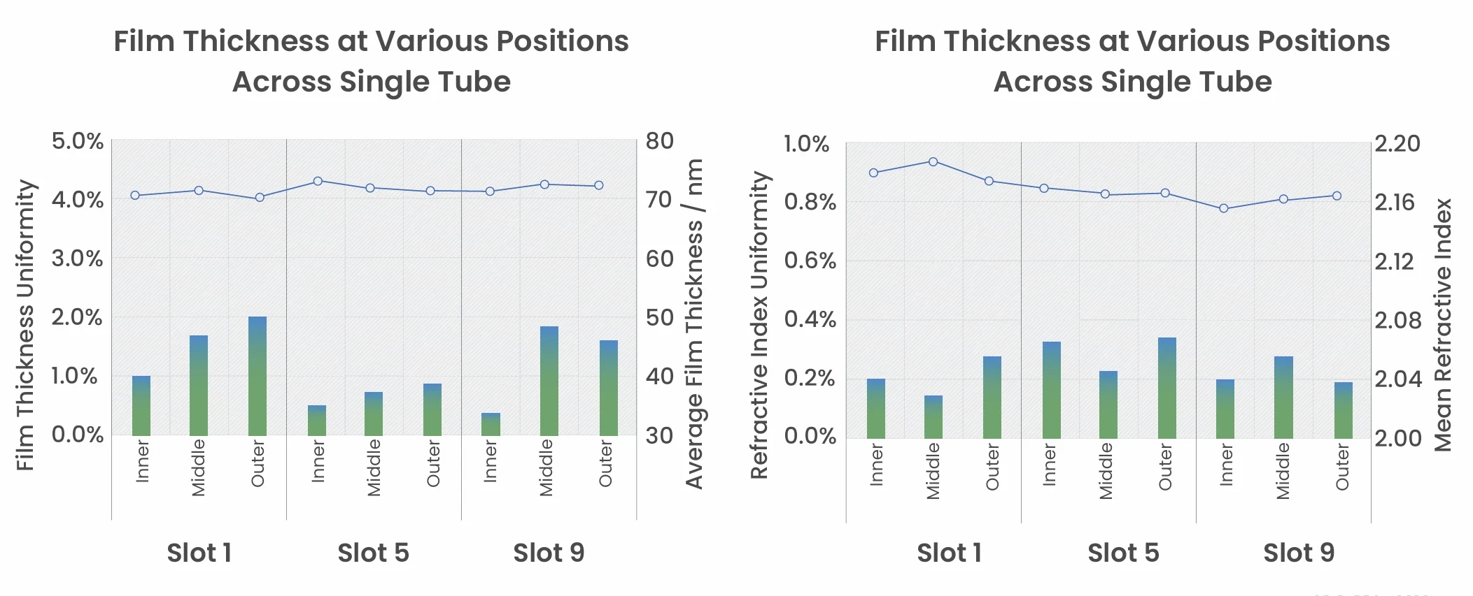
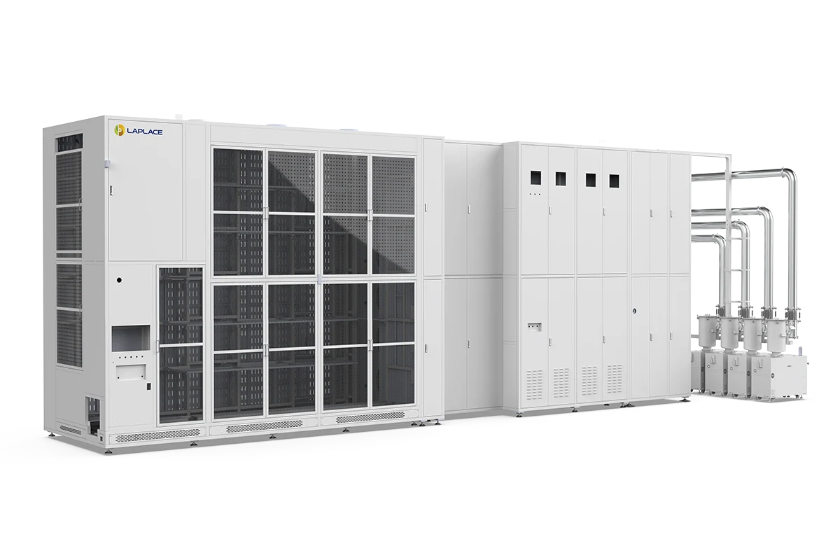
Utilizes plasma to activate gaseous reactants to deposit uniform, dense and functional thin films on substrate surfaces in a low-temperature environment.
1.Plasma-activated reaction: Ionizes reactant gases via RF or microwave methods to generate highly reactive plasma, lowering the reaction activation energy and enabling thin film deposition at low temperatures.
2.Multi-type thin film preparation: Capable of depositing various thin films such as silicon oxide, silicon nitride, silicon oxynitride, and amorphous silicon to meet different functional requirements.
3.Precise process control: Accurately regulates reaction pressure, temperature, gas flow, and plasma power to achieve precise control over film thickness, composition, and density.
4.Uniformity assurance: Optimizes chamber structure and plasma distribution to ensure within-wafer and wafer-to-wafer film uniformity.